Most people are confused with the Nvidia Architecture and naming. In this article, I would like to explain the different Nvidia architecture, graphics cards, and the release timeline.
Also, it’s fascinating to see how much improvement is there in the technology and performance of graphics cards.
Summary – Nvidia Architecture & Graphics Cards
Here are some graphics cards and launch years based on different Nvidia architecture.
- Nvidia Fermi – 400 and 500 series – GTX 480, GTX 470, GTX 580, GTX 570 – Released in 2010
- Nvidia Kepler – 600 and 700 series – Nvidia GTX 680, 670, 660, GTX 780, GTX 770 – Released in 2012
- Nvidia Maxwell – 900 Series – GTX 960, GTX 970, GTX 980 – Released in 2014
- Nvidia Pascal – 1000 series – GTX 1050, 1050 Ti, 1060, 1080 – Released in 2016
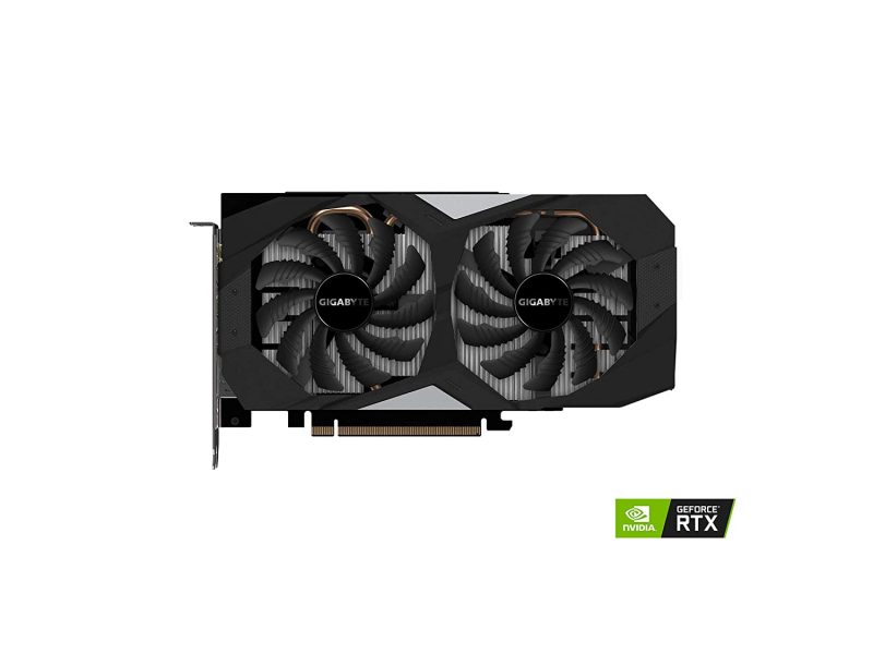
- Nvidia Turing – RTX 2000 and GTX 1600 – GTX 1660, GTX 1650, RTX 2060, RTX 2080 – Released in 2018
- Nvidia Ampere – RTX 3080, RTX 3090, RTX 3070, etc. – Released in 2020
I have been gaming and playing with graphics cards for the last 20+ years. One of the first graphics cards I bought from Nvidia was the GeForce 2 MX-400, released in 2001 (19 years back).
The MX-400 came with just 32 MB of VRAM with a 200 MHz GPU clock speed. It was manufactured using a 180 nm manufacturing process. It was great then but is nothing compared to the computing power that comes with the latest Ampere-based cards like RTX 3080 or RTX 3090.
Let’s look at some of the most recent architectures from the company, starting with Fermi, released in 2010.
Nvidia Fermi vs. Kepler Vs. Maxwell Vs. Pascal Vs. Turing Vs. Ampere
Nvidia Fermi (March 2010)
Nvidia Fermi architecture was released in 2010 (10 years back), and GPUs were based on a 40 Nm manufacturing process.
The Flagship GTX 480 (GF-100) was released in March 2010 and came with DX 11 support. The graphics card has a 1.5 GB GDDR5 VRAM and offers a clock speed of 701 Mhz.
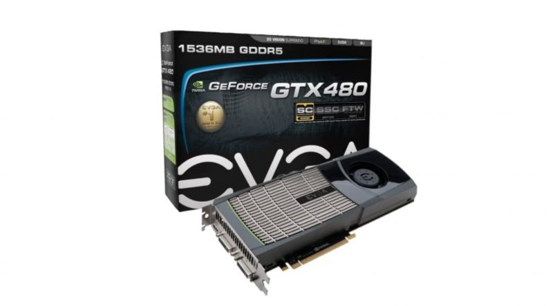
Also, it has a 384-bit memory bus width and offers 3.7 Gbps memory throughput. The GTX 480 came with 3100 million transistors.
Fermi 2.0
Later in the same year, Nvidia launched the GTX 580 based on the 40 Nm manufacturing process but came with the Fermi 2.0 architecture.
Nvidia Kepler ( March 2012)
Nearly two years after the launch of Fermi, Nvidia introduced the new Kepler architecture in March 2012.
The Nvidia Kepler architecture was used in graphics cards such as GTX 680. These new cards were faster and more power-efficient thanks to a further 28 Nm manufacturing process.
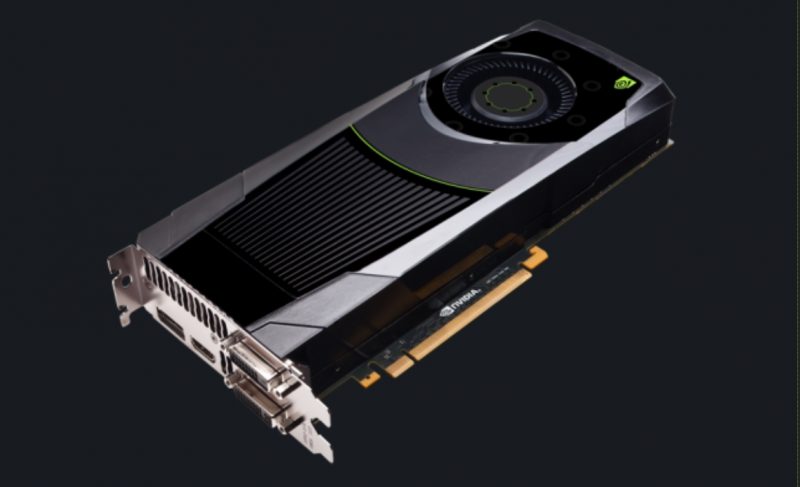
The 28 Nm process from TSMC enabled a significant performance boost over the Fermi. The GTX 680 came with 1006 Mhz clock speed, 2 GB of GDDR5 VRAM, and 6 Gbps memory throughput.
This card’s PSU requirement was just 450 Watts, much less than the GTX 580 or 480, requiring over 600 watts of power.
In 2013, Nvidia introduced the more refined GTX 780 with the same Kepler architecture but several improvements.
The GTX 780 came with 7080 million transistors instead of 3540 million transistors used in the GTX 680.
There were no 800 series of graphics cards from Nvidia, and the company went away from GTX 780 to GTX 980.
Nvidia Maxwell (2014)
The Nvidia Maxwell architecture was released in 2014, and the company launched the 900 Series of graphics cards with it.
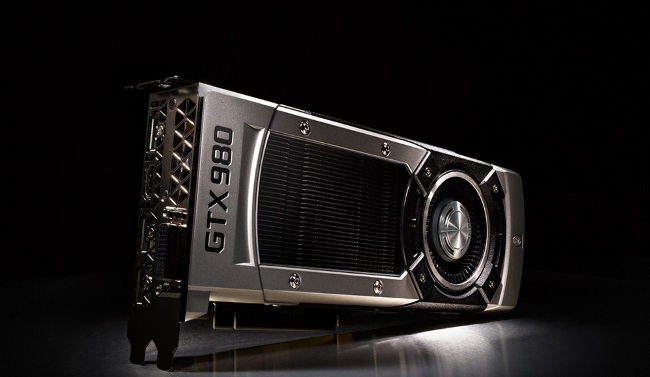
The popular Maxwell-based graphics cards were Nvidia GTX 960, GTX 970, GTX 980, etc.
Maxwell was a big jump for the company as the GTX 980 came with 5200 million transistors and 4 GB of GDDR5 memory.
Maxwell was also based on the TSMCs 28 Nm manufacturing process.
The graphics card came with an 1127 Mhz clock speed, 7 Gbps memory throughput, and incredible gaming performance. With a TDP of just 165 Watts, it offered unmatched performance that was never seen before.
Nvidia Pascal (May 2016)
After a wait of two years, the company released the Pascal architecture-based Nvidia GTX 1080 in May of 2016.
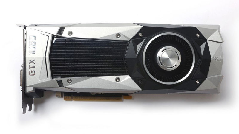
It was another leap for Nvidia, and the graphics card was manufactured using the 16 Nm manufacturing process from TSMC.
The GPU came with 7200 million transistors, 8 GB of GDDR5X VRAM, and 10 Gbps memory throughput. It was one of the most impressive graphics cards and pushed the gaming industry to embrace a 4K resolution.
The card had a boost clock speed of 1733 Mhz and a TDP of just 180 Watts and delivered much more power than the previous generations.
Nvidia Turing (September 2018)
Next, in September 2018, Nvidia released the new RTX 2080 graphics card based on the Turing architecture.
The RTX 2080 came with the new 12 Nm manufacturing process from TSMC and offered 13,600 million transistors.
The Graphics card also came with Ray tracing and tensor cores useful for AI and ML. Further, the RTX 2080 offered 14 Gbps of memory bandwidth, 215 Watts TDP, 8 GB of GDDR6 memory.
Nvidia Ampere (September 2020)
The latest-gen Nvidia graphics cards are based on the Ampere architecture and are released in September 2020.
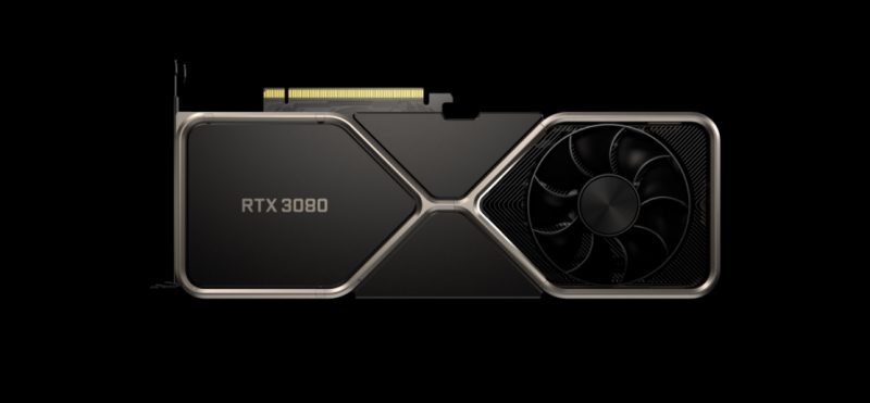
The RTX 3080 is based on an 8 Nm manufacturing process from Samsung. First time in years, Nvidia is not using the TSMC manufacturing process for the graphics cards.
The RTX 3080 has 28,400 million transistors, nearly ten times the GTX 480, and comes with a boost clock speed of 1710 Mhz.
Also, the graphics card has got 10 GB GDDR6X memory with 19 Gbps effective throughput. Also, this new Ampere card draws a lot of power and has 320 Watts TDP.
Also, Read:
- The latest Graphics Cards launched
Can refer to the TechpowerUp GPU Database to check more detailed specs for these graphics cards.